- 您现在的位置:买卖IC网 > Sheet目录280 > 11AA02E48T-I/SN (Microchip Technology)IC EEPROM 2KBIT 100KHZ 8SOIC
11AA02E48
3.0
PRE-PROGRAMMED EUI-48?
The 6-byte EUI-48? node address value is stored in
NODE ADDRESS
The 11AA02E48 is programmed at the factory with a
globally unique, EUI-48? and EUI-64? compatible
node address stored in the upper 1/4 of the array and
write-protected through the STATUS register. The
remaining 1,536 bits are available for application use.
array locations 0xFA through 0xFF, as shown in
Figure 3-2. The first 3 bytes are the Organizationally
Unique Identifier (OUI) assigned to Microchip by the
IEEE Registration Authority. The remaining 3 bytes are
the Extension Identifier, and are generated by Micro-
chip to ensure a globally-unique, 48-bit value.
3.1
EUI-64? Support
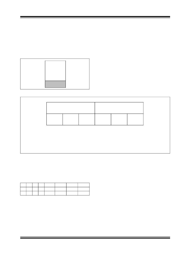
FIGURE 3-1:
MEMORY ORGANIZATION
00h
Standard
EEPROM
C0h
Write-Protected
EUI-48? Block
FFh
The pre-programmed EUI-48 node address can easily
be encapsulated at the application level to form a glob-
ally unique, 64-bit node address for systems utilizing
the EUI-64 standard. This is done by adding 0xFFFE
between the OUI and the Extension Identifier, as
shown below.
FIGURE 3-2:
EUI-48 NODE ADDRESS PHYSICAL MEMORY MAP EXAMPLE
Description
24-bit Organizationally
Unique Identifier
24-bit Extension
Identifier
Data
00h
04h
A3h
12h
34h
56h
Array
Address
FAh
FFh
Corresponding EUI-48? Node Address: 00-04-A3-12-34-56
Corresponding EUI-64? Node Address: 00-04-A3-FF-FE-12-34-56
3.2
Factory-Programmed Write
Protection
In order to help guard against accidental corruption of
the EUI-48 node address, the BP1 and BP0 bits of the
STATUS register are programmed at the factory to ‘ 0 ’
and ‘ 1 ’, respectively, as shown in the following table:
7
X
—
6
X
—
5
X
—
4
X
—
3
BP1
0
2
BP0
1
1
WEL
—
0
WIP
—
This protects the upper 1/4 of the array (0xC0 to 0xFF)
from write operations. This array block can be utilized
for writing by clearing the BP bits with a Write Status
Register ( WRSR ) instruction. Note that if this is per-
formed, care must be taken to prevent overwriting the
EUI-48 value.
DS22122A-page 6
Preliminary
? 2008 Microchip Technology Inc.
发布紧急采购,3分钟左右您将得到回复。
相关PDF资料
11LC161-E/P
IC EEPROM 16K SER AUTO 8DIP
1206704-4
FOENC 1U SOLARIUM MTRJ
1301350343
ANGL PWR DIST BX 125V15A 6
1301350372
PORT OUTLT BX W/(2)5-20&(2)L5-20
1301360074
MULTI-TAP W 4FT 12-3-SO 2608PLUG
1301370282
3070-GFI WITH 5' 14/3 CORD
1301380054
OUTLT BOX 4 5-20DUP BLK FLIPLIDS
1301380110
MULTI OUTLT BOX 3 5-20 DUP 3PH
相关代理商/技术参数
11AA02E48T-I/TT
功能描述:电可擦除可编程只读存储器 2K, 256x8, 1.8V MAC Addressable
RoHS:否 制造商:Atmel 存储容量:2 Kbit 组织:256 B x 8 数据保留:100 yr 最大时钟频率:1000 KHz 最大工作电流:6 uA 工作电源电压:1.7 V to 5.5 V 最大工作温度:+ 85 C 安装风格:SMD/SMT 封装 / 箱体:SOIC-8
11AA02E48T-ITT
功能描述:电可擦除可编程只读存储器 RoHS:否 制造商:Atmel 存储容量:2 Kbit 组织:256 B x 8 数据保留:100 yr 最大时钟频率:1000 KHz 最大工作电流:6 uA 工作电源电压:1.7 V to 5.5 V 最大工作温度:+ 85 C 安装风格:SMD/SMT 封装 / 箱体:SOIC-8
11AA02E64-I/SN
功能描述:电可擦除可编程只读存储器 2K, 256X8 1.8V SERIAL EE IND
RoHS:否 制造商:Intersil 存储容量: 组织: 数据保留: 最大时钟频率: 最大工作电流: 工作电源电压: 最大工作温度: 安装风格: 封装 / 箱体:
11AA02E64T-I/SN
功能描述:IC EEPROM 2KBIT 100KHZ 8SOIC 制造商:microchip technology 系列:- 包装:带卷(TR) 零件状态:有效 格式 - 存储器:EEPROM - 串行(带 MAC 地址) 存储器类型:EEPROM 存储容量:2K(256 x 8) 速度:100kHz 接口:UNI/O?(单线) 电压 - 电源:1.8 V ~ 5.5 V 工作温度:-40°C ~ 85°C(TA) 封装/外壳:8-SOIC(0.154",3.90mm 宽) 供应商器件封装:8-SOIC 标准包装:3,300
11AA02E64T-I/TT
功能描述:电可擦除可编程只读存储器 2K, 256X8 1.8V SERIAL EE IND
RoHS:否 制造商:Intersil 存储容量: 组织: 数据保留: 最大时钟频率: 最大工作电流: 工作电源电压: 最大工作温度: 安装风格: 封装 / 箱体:
11AA02UID-I/SN
功能描述:电可擦除可编程只读存储器 2K UNI/O EE Unique ID Upper Quarter S/W
RoHS:否 制造商:Intersil 存储容量: 组织: 数据保留: 最大时钟频率: 最大工作电流: 工作电源电压: 最大工作温度: 安装风格: 封装 / 箱体:
11AA02UIDT-I/SN
功能描述:电可擦除可编程只读存储器 2K UNI/O EE Unique ID Upper Quarter S/W
RoHS:否 制造商:Intersil 存储容量: 组织: 数据保留: 最大时钟频率: 最大工作电流: 工作电源电压: 最大工作温度: 安装风格: 封装 / 箱体:
11AA02UIDT-I/TT
功能描述:电可擦除可编程只读存储器 2K UNI/O EE Unique ID Upper Quarter S/W
RoHS:否 制造商:Intersil 存储容量: 组织: 数据保留: 最大时钟频率: 最大工作电流: 工作电源电压: 最大工作温度: 安装风格: 封装 / 箱体:
